Monday, December 22, 2008

Yum Extender (2.0.4)

The yum tool is one of the most common utilities used to keep Linux up to date.A graphical tool for updating the fedora is Yum Extender. We can install the yum extender using the command
$ yum install yumex
After installation we can run
$ yumex & to launch the yum extender
or we can goto Applications> System tools > yum extender

Useful tabs of yumex are an update tab on the top left then a group view and an o/p view.From first tab we can select/search the package.From the group view tab we can view the packages by their respective groups,like applications , entertainment, education etc.


It can also be used to remove packages. It keeps track of the installed and available packages.Up to 60% it completes the downloading , in case of adding a package, and the rest is for installing the package.Also when a long list is given to it , it does the downloading in the order of size of the packages ( increasing order of size).

Tuesday, December 2, 2008

A new look , a new system, its Fedora 10

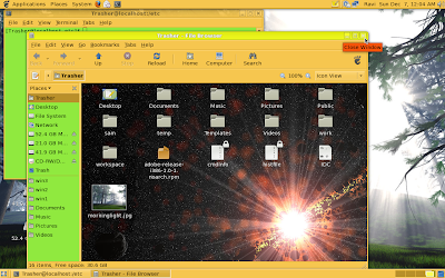
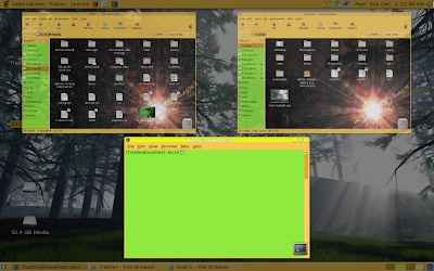
Here is a new look with my Acer aspire 4730Z, using fedora 10.


Even though there was a bug with the fedora 10 it looks fine.The bug is that the network manager and network GUI setting is not changing the subnet mask Then we change the subnet mask in GUI.The bug can be fixed manually by disabling the network manager from System>administration>services
Become substitute user(su) and login as root, then goto the /etc/sysconfig/networking/profiles/default/
using
cd /etc/sysconfig/networking/profiles/default/

edit the file ifcfg-eth0 using gedit or any other editor

gedit ifcfg-eth0

it looks like this
# Realtek Semiconductor Co., Ltd. RTL8111/8168B PCI Express Gigabit Ethernet controller
DEVICE=eth0
BOOTPROTO=none
HWADDR="mac"
ONBOOT=yes
NM_CONTROLLED=no
NETMASK=255.255.255.0
IPADDR=192.168.11.130
GATEWAY=192.168.11.123
TYPE=Ethernet
USERCTL=yes
PEERDNS=yes
IPV6INIT=no
add the line in blue text if there is no such text,then save the file and run the binary ifdown eth0 in sbin

/sbin/ifdown eth0
then
/sbin/ifup eth0
now we will be getting the connection.To configure the yum we need to configure the yum.conf file in etc ,if there is a proxy server
add a line
proxy=http://(IP eg:192.168.1.1 etc):port number/

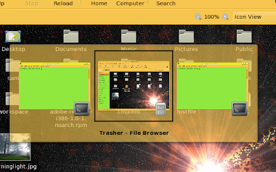
save the file and use yum install something in shell.Use the same settings for wlan to configure Wifi.In fedora 9 the driver for my atheros was not there but for fedora 10 release the driver got automatically installed on upgradation from fedora 9 to fedora 10.Here is a set of pictures from fedora 10, I have configured fedora 10 to look like a new one.


To enable the desktop effects in fedora 10 goto system>preferences>look and feel>desktop effects>enable desktop effects.Use alt+ctrl+arrow keys to rotate the desktop.

Sunday, November 23, 2008

8085 Simulator for Windows (32 -bit)/ Linux

8085sim is a potential product for 8085 microprocessor instruction set simulation.The simulators for both Win(32-bit)/Linux are uploaded hereThe simulator for win is 8085sim.exe and for linux its named as 8085sim.
For Windows :
Copy the 8085sim.exe to any folder named 8085 or anything.It is necessary to copy this to a folder, otherwise the files created by the 8085sim.exe will get scattered around the environment folder.
Run the file
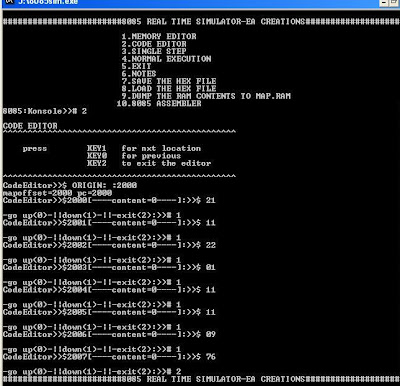
First we will be facing a main menu having 10 options.Select one of them using 1 to 10 numbers.

Code editor(2) & Memory editor (1)
Image above shows the main menu.number 2 is enetered for the code editor we type in the hex code (no need to put H at the end to indicate hex) of the instructions and will at last put a 76H(HLT)instruction.HLT is a must for a program entered in 8085sim.Without an HLT (76H)8085sim will execute infinite loops , so is the case for real hardware.
When we get into the code editor the
Codeeditor>>$ ORIGIN :
comes we have to type in the origin or starting address for the hexcode entry.
After the entry it prints the mapoffset and pc content
For the mem editor the pc will be different than the map offset.
Memory editor provides an interface to direct editing of memory. In this case we can store an array of numbers in some address and use that address in program.

Single step(3) & Normal exe(4)
Image above shows the single stepping mode for 8085sim.After the hexcode entry by using the code editor we can use singlestepping(3) or normal exe(4), for executing the program. When an instruction is executed the 8085sim diaplays all the reg contents below that after showing the instruction and address to which it has been entered.A single stepping or normal exe operation of 8085sim terminated with the execution of a 76 instruction.

Saving the program in harddisk(7)
The above image shows how to save a program that has been entered and executed to harddisk.The 8085 sim sets aside a memory map in RAM of the system ,for virtual 8085simulation.The memory map starts form 0000H to ffffH in hex.So it sets aside 64Kb of memory in RAM . After we leave the simulator it frees the RAM.When its been rerun it will initialise all the contents of RAM to 0H. So we need to write the entered hex code or memory content to hard disk. The purpose of save is to achieve this.We have to enter a file name and also the starting location of the code in memorymap.The saved file is created inside the folder to which the 8085sim was copied.When the file is saved successfully the 8085sim indicates it by printing the number of 8bit codes written to disk
----8-----File written to secondary storage device.
Now we can exit the 8085sim by typing 5.


Loading(8) & Dumping the RAM(9)
The image above shows how to load the file named 16bitadd.Suppose we are exiting the 8085sim by saving the current program.At anytime later on we can try executing the same program by loading that program file into the memorymap of 8085sim.Here the saved file is 16bitadd.
After succussfully loading the file the 8085sim prints a result as shown below.
-----8-----File successfully loaded.
where 8 is the number of code bytes in file.
8085sim also has a memory map analysis file called MAP.RAM. To print the contents of memorymap of 8085sim (0000h to ffffh) select the number 9 from the mainmenu.It dumps the contents of RAM to a file named MAP.RAM.
Assembler is under construction.

For LINUX:
I have tried the binary for Fedora Core 9.If there is any problem please comment.
For linux we have to copy the binary to the bin folder of root.
First open a terminal .Login as a root user
fedora home]$ su
password:
fedora home]#
After the entry as a root the command prompt change from $ to #
copu the 8085sim to /bin
type
home]# cp 8085sim /bin/8085sim
home]#exit
then the 8085sim binary will have entered into the /bin
Now one can type the 8085sim command anywhere to run the simulator.One problem with running the simulator anywhere is that u may not be having enough permissions to create files in some folders.In such cases the save file will show error message .So always use a valid path .Preferably create a folder for 8085simulator.I have created a folder named 8085simfiles in my home directory.
Now change the working directory to home ]$ cd /home/8085simfiles
Now run home]$8085sim
We can see the 8085 mainmenu as shown below


Code editor & Memory editor
Image above shows the main menu.number 2 is enetered for the code editor we type in the hex code (no need to put H at the end to indicate hex) of the instructions and will at last put a 76H(HLT)instruction.HLT is a must for a program entered in 8085sim.Without an HLT (76H)8085sim will execute infinite loops , so is the case for real hardware.
When we get into the code editor the
Codeeditor>>$ ORIGIN :
comes we have to type in the origin or starting address for the hexcode entry. After the entry it prints the mapoffset and pc content.For the mem editor the pc will be different than the map offset. Memory editor provides an interface to direct editing of memory. In this case we can store an array of numbers in some address and use that address in program.


Single step(3) & Normal exe(4)
Image above shows the single stepping mode for 8085sim.After the hexcode entry by using the code editor we can use singlestepping(3) or normal exe(4), for executing the program.When an instruction is executed the 8085sim diaplays all the reg contents below that after showing the instruction and address to which it has been entered.A single stepping or normal exe operation of 8085sim terminated with the execution of a 76 instruction.

Saving the program in harddisk(7)
The above image shows how to save a program that has been entered and executed to harddisk.The 8085 sim sets aside a memory map in RAM of the system ,for virtual 8085simulation.The memory map starts form 0000H to ffffH in hex.So it sets aside 64Kb of memory in RAM. After we leave the simulator it frees the RAM.When its been rerun it will initialise all the contents of RAM to 0H. So we need to write the entered hex code or memory content to hard disk. The purpose of save is to achieve this.We have to enter a file name and also the starting location of the code in memorymap.The saved file is created inside the folder to which the 8085sim was copied.When the file is saved successfully the 8085sim indicates it by printing the number of 8bit codes written to disk
----8-----File written to secondary storage device.
Now we can exit the 8085sim by typing 5.
Loading(8) & Dumping the RAM(9)
The image above shows how to load the file named 16bitadd.Suppose we are exiting the 8085sim by saving the current program.At anytime later on we can try executing the same program by loading that program file into the memorymap of 8085sim.Here the saved file is 16bitadd. After succussfully loading the file the 8085sim prints a result as shown below.
-----8-----File successfully loaded.
where 8 is the number of code bytes in file.


8085sim also has a memory map analysis file called MAP.RAM. To print the contents of memorymap of 8085sim (0000h to ffffh) select the number 9 from the mainmenu.It dumps the contents of RAM to a file named MAP.RAM.Assembler is under construction.

Saturday, November 22, 2008

How to remove abk.bat virus

Goto start>run>regedit
delete the entry
HKCU\Software\Microsoft\Windows\CurrentVersion\Run kamsoft
then reboot to another os preferably linux or to same system
delete all autorun.inf files made by the abk.bat infection
delete all abk.bats from all drives.
We cannot see the file unless we make all hidden files unhidden.
To enable the folder options >view>show hidden files and folders radiobutton
goto HKlocal machine>software>microsoft>windows>current version>explorer>advanced>folder>hidden>showall>click on checkedvalue and make its value 1
Then untick the hide protected os files in folderoptions >view
now the abk.bat files will be visible delete all of then including autorun.inf

Friday, November 14, 2008

Ultra dense non volatile memories using memristors

The memristor was first proposed by a scientist named LEON O.CHUA in 1971 as a fourth fundamental circuit element. The existence of such an element was mathematically proved and the theoretical properties were predicted using mathematical equations. But it was only in April 2008 the scientists were able to came up with a physical model to prove it.
Why the name memristor
By definition a memristor is characterized by a relation of the type g(Ψ, q)=O. It is said to be charge-controlled (flux-controlled) if this relation can be expressed as a single valued function of the charge q (flux-linkage Ψ). The voltage across a charge-controlled memristor is given by

v(t) = M(q(t)) . i(t)
where

M(q) = d Ψ(q)/dq.

Since M(q) has the unit of resistance, it will henceforth be called the incremental memristance. The value of the incremental memristance at any time to depends upon the time integral of the memristor current (voltage) from t = - ∞ to t= to. Hence, while the memristor behaves like an ordinary resistor at a given instant of time to, its resistance) depends on the complete past history of the memristor current. The memory property of the memristor arises from this fact. It is interesting to observe that once the memristor voltage v(t) or current i(t) is specified, the memristor behaves like a linear time-varying resistor.

Thus while behaving like an ordinary resistor at any given instant of time t0, its resistance depends on the complete past history of the memristor current. Thus memristor is basically a charge dependent resistor. Since memristance is a function of charge which is the time integral of current, the memristor behaves like a nonlinear resistor. The equation v(t) = M(q) . i(t) gives linear relationship only when M(q) is constant. Constant M(q) means charge does not vary with time. But a nonzero current results in instantaneously varying charge. Thus M(q) results in a nonlinear relationship. Thus memristor has meaning only in nonlinear ckt.
Device structure and fabrication


Single-crystalline TiO2 was used to elucidate how the metal/oxide interfaces control the device resistance. As shown in Fig. 1a, a single crystal of rutile TiO2 (bandgap Eg =3.0 eV) was first annealed in a 95% N2 and 5% H2 gas mixture at 550 °C for 2 h to create an oxygen-deficient layer near the surface. Oxygen vacancies in TiO2 are known to act as n-type dopants, transforming the insulating oxide into an electrically conductive doped semiconductor. Metal/semiconductor contacts are typically ohmic in the case of very heavy doping, and rectifying (Schottky-like) in the case of low doping. Two pairs of 100 µm x 100 µm Pt and Ti electrode contact pads were deposited onto the single crystal, as shown schematically in Fig. 1a: pads 1 and 4 were Pt films (80 nm thick) and pads 2 and 3 were Ti films (5 nm thick) with Pt (80 nm thick) caps. The 5-nm Ti layer was used as a chemically reactive contact to further reduce the TiO2 and create a locally high concentration of oxygen vacancies close to the metal/ semiconductor interface. These two regions showed an ohmic contact with resistance ~ 40Ω, showing that the bulk resistance of the annealed single crystal was low. In contrast, the electrical resistance between the two chemically unreactive Pt contact pads 1 and 4 was four orders of magnitude higher than the others.


Memory Storage

The bipolar switching behavior of the nanoscale metal/metal oxide/metal memristors can be used to develop resistive non volatile RAMs (Re-NVRAMs). The researches and experiments are indicating that the memristor based Re- NVRAMs will be faster than the evolving memory technologies like MRAM, PCRAM etc and 100x times faster than flash memory. Also the scientists at HP have created an ultra high density crossbar switches, which use thin film memristors to pack a record 100Gbits per cm² in a single die compared to the 16Gbits for the highest density flash memory chips extant. The memristors made by HP are very small about 15nm.

HP memristor based RRAMs will be using the crossbar architecture. Metal lines spaced less than 50-nm apart will serve as the bottom electrodes with the top electrodes patterned from metal lines arranged perpendicular to the bottom lines into a crossbar switch. In between the metal lines twin layers of titanium dioxide is sandwiched --one doped with oxygen vacancies and the other undoped. Running current between two metal lines--one on the top and one on the bottom--the device will be able to address individual bit cells, changing their resistance and thus turning bits on and off.

Ø Reading: The reading operation can be performed simply by applying a voltage lower than the threshold voltage. If the memristor is on then it will conduct even at the threshold voltage. If off it will not conduct. Thus binary data can be read.

Ø Writing: The writing operation can be performed by applying a voltage greater than the threshold voltage to write 0( or 1 depending upon the configuration) by making the memristor ON. To write a 1 (or 0) a voltage of opposite polarity whose magnitude is greater than the threshold voltage is applied which turns the memristor OFF.

Ø Addressing: Metal lines are arranged in two layers like rows and columns which are perpendicular with the other and are separated by the thin semiconductor film. Running current between the metal lines- one on the top and one on the bottom- the device will be able to access individual bit cells, changing their resistance and thus turning bits ON and OFF.

Advantages of Memristive memory

Ø For the memristor based memories there is no need of refreshing the data as in the case of today’s DRAMs. This could drastically reduce the power consumption.

Ø The inductive and capacitive effects associated with the memristors are negligible. This eliminates the delays due to charging time, storage time, discharging time.

Ø The memristive behavior and speed is inversely proportional to the square of device size. So scaling down increases the performance by great extent.

Ø The memristors can packed at a very large density than transistors. 15nm memristors are made which can hold 100Gbits/cm². Even at 4nm, a square centimeter of memristor can hold one terabit ie 10¹² bits/cm².

Ø Analog data storage is possible under controlled operation.

Saturday, October 25, 2008

Quantum Well FET(QWFET)

Quantum mechanical effects become important when device geometries are scaled down to nanometer range. In ultra deep submicron regime, quantum mechanical effects can be a show stopper for device integration. InSb QWFET is a device utilizing the high mobility of InSb. InSb QWFET based circuits will consume less power and ultra high switching speeds can be achieved using it.
The quantum well transistor architecture employs barrier layers with higher band-gap materials to mitigate the effect of the narrow band-gap InSb on device leakage and breakdown.The transistors were fabricated on a semi-insulating GaAs substrate using a relaxed metamorphic buffer layer of AlyIn1-ySb to accommodate lattice mismatch, a compressively strained InSb quantum well confined between layers of AlxIn1-xSb and a Schottky barrier metal gate. High speed carrier transport occurs in the low band-gap InSb quantum well (QW). The buffer layer is made of AlkIn1-kSb, with the indium concentration graded so that it can match the lattice constant of both the GaAs substrate and the InSb channel.

The high speed of operation is achieved using the material property of InSb as well as the property of quantum wells.InSb is known to be the greatest mobility semiconductor. A remote doping concept is used to get ride of the impurity scattering.An extractive technology (substrate bias with potential hill)is used to extract the thermally generated carriers so that the device can be operated at room temp.

For high speed direct coupled FET logic (DCFL) applications, both enhancement (i.e. positive VT) and depletion mode devices are required. An enhancement mode InSb QWFET is demonstrated for the first time using a deep recess etch in the gate region, which shows a peak fT of 305GHz at 0.5V VDS. A depletion mode device is demonstrated at the same time utilizing a shallow recess gate with a peak fT of 256GHz at 0.5V VDS. The demonstration of both high performance depletion and enhancement mode InSb QWFETs makes the technology a promising candidate for future high speed, low power logic applications. Enhancement device achieve record intrinsic speed of 305GHz .The record speed of the enhancement device is due to the deep recess etch. The deep recess etch increases the gate control of the device as described by the MOSFET ID(sat) equation. Recessed gate architecture improves the gate field to quantum well coupling, improving scalability. Scalability further increases by buffer p-type doping.

Sunday, September 21, 2008

Learning VerilogHDL

There are several ways of representing digital logic.One method employed to simplify the complexity in transfering the schematic representations is to use HDLs(hardware description languages).One popular one is Verilog HDL. Although there are no packages and libraries available in Verilog ,its simpler because of its similarity in format compared to C language.Note that the C is a sequntial laguage running on sequential device ,while the Verilog is a HDL which is only for the hardware! its not a programming language!
Another great thing about this Verilog is that it allows various levels of abstraction
We can have a structural style a data flow style or a behavioural style!The Verilog HDL is an event driven one.(assuming fedora, am in fedora9)We require a open source tools such as cver and gtk wave for simulation and result.gtk wave is a waveform viewer.There are many more tools available.
The basic functional block in Verilog is the "module"
A typical module statement may look like module halfadder(A,B,S,Cout);
where the A,B,S,Cout are the input and output list of a half adder


The code for generating a half adder is shown
(open any editor,vim ,gedit ,any edit type the following code)
module halfadder(A,B,S,Cout);
input A,B;
output S,Cout;
xor x1(S,A,B);//since this is a primitive we cannot specify the portlist as we wish
//the format is output followed by input
and a1(Cout,A,B);
endmodule
we save this as a file (say) ha.v
The above specified code is a structural description of half adder.after creating this we have created a half adder in verilog. This can be given to the synthesis tool.For varification of the logic of the ckt we need testbenches to be written .

`timescale 1ns/1ps
`include "ha.v"
module ha_tb;
reg A_t,B_t;
wire S_t,Cout_t;

halfadder UUT(.A(A_t),.B(B_t),.S(S_t),.Cout(Cout_t));
initial
begin
$dumpfile("ha.vcd");
$dumpvars(2,ha_tb.UUT);
end

initial
begin
A_t=1'b0;
B_t=1'b0;
#5 A_t=~A_t;
#5 B_t=~B_t;
#5 A_t=~A_t;
end
initial
#30 $finish;
endmodule


after saving this in another name ha_tb.v,we can simulate the half adder with the help of test bench and cver writing
user$]cver ha_tb.v to the terminal .Then it will generate a value change dump file called ha.vcd in the same directory which can be opened through GTKwave for viewing the simulation result!


Saturday, August 9, 2008

MAGNETIC DOMAIN RACETRACK MEMORY

Fig.1.

Fig. 1. The racetrack is a ferromagnetic nanowire, with data encoded as a pattern of magnetic domains along a portion of the wire. Pulses of highly spin-polarized current move the entire pattern of DWs coherently along the length of the wire past read and write elements. The nanowire is approximately twice as long as the stored DW pattern, so the DWs may be moved in either direction. (A) A vertical-configuration racetrack offers the highest storage density by storing the pattern in a U-shaped nanowire normal to the plane of the substrate. The two figures show the magnetic patterns in the racetrack before and after the DWs have moved down one branch of the U. past the read and write ele­ments, and then up the other branch. (B) A horizontal config­uration uses a nanowire parallel to the plane of the substrate. (C)Reading data from the stored pattern is done by measuring the tunnel magnetoresistance of a magnetic tunnel junction element connected to the racetrack. (D) Writing data is accomplished, for example, by the fringing fields of a DW moved in a second ferromagnetic nanowire oriented at right angles to the storage nanowire. (E) Arrays of racetracks are built on a chip to enable high-density storage.

RM is fundamentally a shift register in which the data bits (the DWs) are moved to and fro along any given racetrack to intersect with individual reading and writing elements integrated with each racetrack.Permalloy is the term for a nickel iron magnetic alloy. Generically, it refers to an alloy with about 20% iron and 80% nickel content. Permalloy has a high magnetic permeability, low coercivity, near zero magnetostriction, and significant anisotropic magnetoresistance.

Advantages of racetrack memory over the other types of memory

Alternative for HDDs and existing solid state memories except SRAM.

100 times bits/area than SRAM

Greater operating speed and less power consumption

Can be 3D.

can replace the current architecture of memory in computers

Friday, August 1, 2008

MOSFET SCALING

High K Metal Gate Technology (HKMG)

Dielectric leakage problem

Dielectric leakage is problem faced during scaling the MOSFET
This happens because of the tunneling of the electrons through the thin dielectric
As the width(physical) of the dielectric reduces leakage becomes more due to tunneling

High K Solution

The problem however can be overcome by the usage of High K dielectric.This shows that the ,material must be electrically thin but physically thick(Hafnium oxide ).For the same capacitance the oxide thickness of the high K dielectric (oxide) can be more .


Problem with the polysilicon gate
  • Polysilicon depletion
  • Need for enhanced channel mobility

Potential solution

No depletion, very low resistance gate, no boron penetration, compatibility with high-k
Also lesser phonon scattering, hence enhanced mobility

Thursday, June 12, 2008

SIMPLE LCD USAGE THROUGH PIC C

PIC C is a c compiler for pic microcontrollers (described earlier for my iROOM)

Here is a simple "hello world" fprogram for the pic 16f877A

#include <16f877a.h> //Must be included
#use delay(clock=16000000) //for specifying the clock frequency in Hz

#include


void main()
{
lcd_init();


/*******************************************************************************/
//PRINTING "HELLO WORLD" IN LCD
/*******************************************************************************/


lcd_putc("\f HELLO WORLD \n");


// \f Clear display
// \n Go to start of second line
// \b Move back one position


}

Sunday, June 1, 2008

TDA7267 Mono Audio Amplifier

APPLICATION circuit
The device TDA7267 is a new technology Mono Audio Amplifier in MINIDIP package specifically designed for TV application.Thanks to the fully complementary output configuration the device delivers a rail to rail voltageswing without need of boostrap capacitors.
APPLICATION HINTS:
For 12V supply and 8W speaker application, its
maximum power dissipation is about 1W.

Friday, April 4, 2008

Electronic Circuits That Bend and Stretch


The new circuits, developed by a team of researchers at the University of Illinois at Urbana-Champaign led by Professor John A. Rogers, are built from ribbons of silicon only a few nanometers thick that are mounted on flexible plastic substrates.


SHRINK, WRAP: : This circuit sheet [LEFT] has not aged rapidly. The wrinkles make it possible to stretch the sheet over a sphere or an irregularly shaped object without breaking the sheet or damaging its current-conducting structures. To wrap circuits around a rod as thin as a strand of hair [RIGHT], the researchers made them superthin.
for more details click here

Tuesday, April 1, 2008

Automatic light intensity control system and state identification


The block diagram explains the basic system design. Driver used is MAX 7219.The driver is controlled by a PIC (not necessarily PIC). The driver reduces complexity of work associated with the individual basia required for the LEDs. The driver however can drive 64 LEDs and conmsumes only 160mA at 5V. Thus its a great promise for the future lighting solutions.

i-Room is a state-of-the-art, self-configuring lighting control system solution for bedrooms, offices and perimeter areas. Under automatic operation, the system senses luminosity inside and outside a room, dims the LED’s to maintain a prescribed level of illumination inside the room. i-Room is an smart system that saves energy by keeping unoccupied cells of a large room unlit and maximizing the use of available natural light inside the room. By operating on a feedback loop where the system senses light and the presence of people, the system makes smart decisions on how to best illuminate the space according to presence of people and control the brightness according to ambient light. The project is very expandable and versatile. The heart of the system is the state synthesizer PIC 16F883 which is an 8 bit CMOS microcontroller. The sensors of the system are LASER-LDR pair that is available and can be set up easily. In the long-run, i-Room provides control solutions that reduce energy costs and extend lamp life.

i-ROOM is a simplified version of systems and equipments sold at high prices in the high-income housing segment as well as high-visibility public buildings. With improvements, i-ROOM could also be used in architecture projects to enhance prototypes and models of buildings.

STATE OF ART TECHNOLOGY HISTORY

There are available at least two broad categories of automatic lighting control systems for rooms. Automatic lighting control systems falling into the first broad category consist of a plurality of discrete, self-contained automatic lighting control modules which operate essentially independently of one another for controlling the lighting conditions in respective separate sections of a large room. Automatic lighting control systems falling into the second broad category employ a network of sensors for detecting the illumination levels and/or presence of persons in each part of the room and a programmable central controller which analyzes the sensor feedback signals in accordance with a lighting control program, and outputs control signals to adjust the lighting levels of the monitored regions of the room in accordance with the lighting control program. In this connection, automatic lighting control modules in each part of the room are operated under the control of the programmable central controller. Thus, rather than operating independently of one another, the distributed modules are functionally integrated into a single room-wide network under the control of the programmable central controller. …………………

In the type of system of first category, each light source is provided with an automatic control device which includes a presence detector (e.g., a motion detector or a passive infra-red detector) and a light intensity detector (e.g., a photocell detector). In operation, each automatic control device functions to switch its corresponding light source on when an occupant is detected in its localized area of coverage and to vary the intensity (brightness) of the light produced by its corresponding light source in response to variations in the sensed ambient or background light level in its localized area of coverage. In this manner, adequate lighting is provided in all occupied areas despite variations in the ambient lighting conditions present in various zones of the room.

Another way of implementing system includes one or more individual dimming controllers each of which controls the light intensity (brightness) of one or more light sources in a room or localized area of the building which is lit by internal light and external light. In particular, each dimming controller adjusts the intensity of the internal light in dependence on the external light intensity, which varies with the time of day and atmospheric conditions. The intensity and direction of the external light is sensed by external light sensors. Each of the light sources in the various sections of a large room can be provided with an individual dimmer, to thereby enable the intensity of the different light sources to be individually adjusted in such a manner as to provide either a uniform or non-uniform light intensity profile. In general, the light intensity of the internal light is controlled in substantially inverse dependence on the external light, e.g., when the external light decreases the light inside the room is made brighter.

A more advanced automatic lighting control system of the first category developed so far is a programmable illumination system which includes a plurality of individual illumination units each of which is provided with a programmable controller which functions to automatically adjust the light level of its associated illumination unit to a prescribed (programmed) light output level for each of a plurality of different illumination modes. Such an illumination system has particular utility in a space, such as a living room, offices, or shop, in which various different tasks which require different lighting conditions are to be performed. An illumination mode is defined as a particular setting of the light output levels of all illumination units in a particular illumination area for providing a desired illumination profile for a particular task to be performed (or desired ambience) in that particular illumination area. After initial programming of the system, the system automatically adjusts the output levels of the individual illumination units to the proper level for a selected illumination mode.A wireless or hard-wired remote controller can be utilized to program each of the individual illumination units of the system.

The automatic lighting control system of the second category developed includes a programmable microprocessor-based central controller which is responsive to feedback signals produced by a network of presence and light sensors distributed throughout various sections of a room to automatically control the light output levels of lighting units in different zones of the room. The system is equipped with an override feature to enable room occupants to override one or more of the automatic lighting features of the system, e.g., to enable the lights to be turned off, despite the sensed presence of people in a room. For example turning off lights for the operation of an overhead projector (OHP).

A more advanced automatic lighting control system of the second category includes a plurality of illumination sensors distributed throughout the building, but advantageously not necessarily in a one-to-one relationship to the light sources distributed throughout the room. In this connection, a generally lesser number of illumination sensors than light sources are strategically placed inside (and outside, if desired) of the room in order to provide a non-redundant set of measurements of internal illumination. These measurements are then collectively processed by a central automatic control device which preferably includes a neural network or a fuzzy logic unit. The automatic control device is programmed with a set of inference rules chosen to meet user-defined comfort and/or energy efficiency criteria. In operation, the automatic control device automatically controls the light output levels of the light sources throughout the room in accordance with the user-defined inference rules to thereby meet the user-defined comfort and/or energy efficiency criteria. Various user-selectable customized usage modes can be programmed to enable room occupants to vary the general lighting conditions in a selected or area(s) of the room in accordance with various usage requirements by merely selecting the appropriate usage mode desired by the occupants of the room.

A major shortcoming of all presently known automatic lighting control systems is that none of them are designed to optimize the energy efficiency of a room lighting system for a target energy consumption level and a prescribed set of lighting system usage parameters and constraints. Thus, there exists a need in the art for an automatic lighting control system which overcomes this and other limitations, disadvantages, and shortcomings of the presently known automatic lighting control systems.

PRESENT SITUATION

Presently methods for optimizing the energy efficiency of a lighting system which includes a plurality of light sources, which includes the steps of defining a set of parameters for the lighting system, and using a linear programming technique, taking into account the set of parameters, to produce energy allocation output data which satisfies a total energy consumption constraint that the total energy allocated to the lighting system not exceed a target energy consumption level, and which is representative of an optimal allocation of energy to each of the light sources. The lighting system is installed in a room which includes a plurality of sections each of which is equipped with light sources.

In general, the lighting optimization problem is translated into a linear programming problem by formulating a set of lighting system energy allocation constraints, converting these constraints into a set of constraint equations and a cost function, converting the constraint equations into a set of simultaneous linear equations, and then solving the set of simultaneous linear equations in such a manner as to minimize the cost function, to thereby produce the energy allocation output data, which is preferably in the form of an optimal brightness level for each light source. These steps are preferably implemented in computer software, which is preferably loaded in a programmable central controller of an intelligent lighting control system which is responsive to the energy allocation output data for automatically adjusting the brightness level of each of the light sources to the optimal brightness level.………………………………………………………………….

Preferably, available energy remaining after satisfying minimum brightness levels for each zone in the room is allocated at least partially on the basis of the designated priority level of each room, and/or the energy efficiency of the light sources. Further, zones of equal priority are preferably allocated an equal amount of available energy. Also, the method preferably includes a post-processing filtering step for determining whether the optimal brightness level for each zone is equal to a minimum brightness level, and, if not, adjusting the optimal brightness level for the zone to the minimum brightness level.


The terms "room", and "light source" can be used in their broadest possible sense. For example, the term "room" can be intended to encompass any structure which has a lighting system, including, but not limited to, single-family homes, multi-family dwellings, apartment buildings, office buildings, warehouses, factories, gymnasiums, auditoriums, theaters, museums, shops, restaurants, hotels, shopping malls, and indoor stadiums. The term "room" is intended to encompass any identifiable, separately lighted portion, zone, sector, or localized area of a building, including, but not limited to, conventional rooms such as offices, bathrooms, closets, storage areas, factory floors, basements, conference rooms, foyers, common areas, utility rooms, or any associated set of such separately lighted portions or zones, sectors, or localized areas of the building whose lighting is intended to be commonly controlled. The term "light source" is intended to encompass not only individual lamps, but also any associated set or group of lamps which are intended to be commonly controlled, e.g., all of the lamps associated with a given room in the building.


Tuesday, February 5, 2008

State identification program for the iRooM project

ROOM SETUP The room setup required for the implementation of the state identification is as shown above. The partitions can be done logically using the LASER -LDR,LASER-Phototransistor,or IR -sensor pairs .

The room is divided into three cells named C0 C1 and C2. S0, S1 and S2 are state variables that store the present state of the cell (i.e. state is 1 if people are present in the cell and 0 if cell is vacant). A small region near the door is assigned a state variable S3.

It is an intermediate state that is used to determine entry into and exit from the room. L0, L1, L2, L3, L4, L5 are the sensors placed in the room to determine the transition of people across the room through various cells. This is necessary to determine the present state of each cell so as to do automatic lighting up of an LED array provided in each cell if count of people is the cell is greater than zero. The LED array in each cell is OFF if the cell is empty.

STATE SYNTHESIZER

The automatic lighting system control is implemented with the help of a state synthesizer, which generates the next state with the help of present state and sensor inputs. A program is written and the artificial intelligence is created by burning that program into the microcontroller that emulates the function of a state synthesizer.The state transitions are detected by the sensor inputs and past states. The output of the state synth is the state itself hence its a moore one.

Sunday, January 27, 2008

Programming the PIC in C/PIC C

First thing is to find a help file located anywhere in the compiler development environment .Then we have to understand the basic data types .Then the most important part in pic C programming is to understand the built-in functions and the port directives like" poke "in PICbasic .Then we have to write the code in the development environment,including the basic header files .For example in case of the picc compiler we may be including the "16f877.h",if we are using the 877 pic of the 16f series.but there is no such option in micro c as well,instead it requires some project file initialization i think!!
For the demonstration purpose i have written a code to make pinA0 high if pinB0 is high and then push pinA1 low.Else if the pinB0is low the pinA0must be 0 and pinA1must be 1. During this time the pinC0 will blink with a delay of 500ms
the code is given below